Since this project involves many firsts for me, I decided to keep the features at the minimal bar - this means no USB OTG, no properly filtered analog references, no RTC. One goal however is to reach 120 MHz which means we’ll need a crystal!
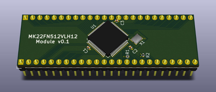
Here’s a render of the final board sent to OSH Park:
Tips from Teensy 3.1
The Teensy isn’t open-hardware/open-source but it does have some rough schematics that proved extremely helpful.
The most closed part of the Teensy is the programmer/bootloader running on the Mini54 MCU on the Teensy board. PJRC sells these chips, pre-programmed, to allow users to make custom Teensy boards. The “Crystal Guidelines” and “Troubleshooting” section on their page has really great info to get us started.
Breadboard Friendly-ness
Similar to the Teensy, I wanted the breakout in a dual-inline PCB package that you could drop onto a breadboard. Unlike the Teensy, however, I wanted to expose as many pins as possible.
With the additional pins, the resulting board will to be much longer than the Teensy - which is great because it provides more room for routing signals. This, plus the fact that I’ve only laid out two PCBs before, made me settled on a 2 layer design - instead of a 4, like the Teensy.
In order to fan out all the signals from the MCU, I had to rotate the chip 45 degrees. This made the PCB a little bit wider than the Teensy but I love the look :)
This made the PCB a little wider than the Teensy and the end packages was 48-pin dual-inline package. It’s 8 pins wide which means on a typical breadboard you’ll have 2 free pins on each sides.
Isolating the Crystal
I choose a 16 MHz crystal with a 9pF load capacitance, similar to the Teensy. The low load capacitance means the internal, programmable, load capacitors should suffice - else we would have to add two external capacitors. I went with 16 MHz to match the Teensy but 4, 8 and 32 MHz are also good choices.
Without any external load capacitors or a feedback resister, we’re forced to run in low-power/low-gain mode (see Section 26.5). With this setup, it’s vital to keep the crystal and related traces free of noise and interference.
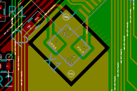
To keep the traces short, I kept the crystal as close to the XTAL pins as physically possible and gave it an independent ground plane connected to the ground pin right next to the XTAL pins. The ground plane skirts the crystal as well as shield it’s underside via the bottom layer.
Pull Ups, Tie Ups and Tie Downs
In order to boot and avoid faults, there’s a few special pins you’ll need to connect to the rails. Section 5.2 has some recommendation for us.
RESET_b and EZP_CS_b (PTA4)
There are two pins we need to pull up in order to boot. RESET_b is an active low reset pin - pretty self explanatory. During reset, holding EZP_CS_b low causes the MCU to boot into EzPort mode (one of the flash programming modes available). Holding the pin high causes MCU to boot into the programmed flash. We’re going to be using the EzPort to program the flash so we’ll pull this pin up instead of typing it up.
VOUT33 and VBAT
VOUT33 is the output pin for the internal 3.3V regulator but we’ll be supplying our own 3.3V so we can tie this pin to VDD. VBAT is the backup battery into for the RTC circuitry and since we’re not planning to use the RTC, we’ll leave this floating - we’ve to be careful thou, without power supplied, accessing the RTC memory mapped registers can cause the core to lock up.
VDDA/VSSA and VREFH/VREFL
VDDA+VSSA are the supply rails for the ADC/DAC and VREFH+VREFL are the reference voltages. In a well designed board these will be tied to our sources through an inductor (low pass) with a bypass capacitor close by. We’re not really worried about having clean signals here so just tie them to our rails!
Files
- Schematic (PDF)